Enhance a problem solving ability in Physics for various competitive and qualifying examinations like GRE, GATE, CSIR JRF-NET, SET, UPSC etc.
Notice
electronic
The Boolean expression $B\cdot(A+B)+A\cdot(\bar B+A)$ can be realized using minimum number of
1 AND gate
2 AND gates
1 OR gate
2 OR gates
\begin{align*}
{}&{}B\cdot(A+B)+A\cdot(\bar B+A)\\
&=B\cdot A+B\cdot B+A\cdot\bar B+A\cdot A
\end{align*}
But $ B\cdot B=B$ and $ A\cdot A=A$
\begin{align*}
{}&{}B\cdot(A+B)+A\cdot(\bar B+A)\\
&=B\cdot A+B+A\cdot\bar B+A\\
&=B\cdot(A+1)+A\cdot(\bar B+1)
\end{align*}
But $A+1=1$ and $(\bar B+1)=1$
$$B\cdot(A+B)+A\cdot(\bar B+A)=B+A$$
Hence answer is (C) 1 OR gate
Consider the digital circuit shown below in which the input $C$ is always high (1).
The truth table for the circuit can be written as
A
B
Z
0
0
0
1
1
0
1
1
The entries in the Z column (vertically) are
1010
0100
1111
1011
AND gate has output high when both inputs are high, OR gate has output high when any one or both inputs high and EXOR gate has high output when any one input is high but not both inputs hight.
Hence, answer is (D)
A resistance is measured by passing a current through it and measuring the resulting voltage drop. If the voltmeter and
the ammeter have uncertainties of 3% and 4%, respectively, then
The uncertainty in the value of the resistance is
7.0%
3.5%
5.0%
12.0%
The uncertainty in the computed value of the power dissipated in the resistance is
7%
5%
11%
9%
If $\Delta x$ and $\Delta y$ are uncertainties in measurements of $x$ and $y$, then uncertainty in $z$ i.e. $\Delta z$, for different cases
is given by
\begin{eqnarray}
\begin{array}{cc}
{\scriptstyle z=x\pm y }&{\scriptstyle\Delta z=\sqrt{(\Delta x)^2+(\Delta y)^2}}\\
{\scriptstyle z=xy} &{\scriptstyle\Delta z=|xy|\sqrt{\left(\frac{\Delta x}{x}\right)^2+\left(\frac{\Delta y}{y}\right)^2}}\\
{\scriptstyle z=\frac{x}{y}} &{\scriptstyle\Delta z=\left|\frac{x}{y}\right|\sqrt{\left(\frac{\Delta x}{x}\right)^2+\left(\frac{\Delta y}{y}\right)^2}}\\
{\scriptstyle z=x^n} &{\scriptstyle\Delta z=\left|n\right|x^{n-1}\Delta x}\\
{\scriptstyle z=f(x,y)} &{\scriptstyle \Delta z=\sqrt{\left(\frac{\partial f}{\partial x}\right)^2(\Delta x)^2+\left(\frac{\partial f}{\partial y}\right)^2(\Delta y)^2}}\\
\end{array}
\end{eqnarray}
In our case $\Delta V=3\%$ and $\Delta I=4\%$, as $R=\frac{V}{I}$
\begin{align*}
\Delta R&=\left|\frac{V}{I}\right|\sqrt{\left(\frac{\Delta V}{V}\right)^2+\left(\frac{\Delta I}{I}\right)^2}\\
&=\left|\frac{100}{100}\right|\sqrt{\left(\frac{3}{100}\right)^2+\left(\frac{4}{100}\right)^2}\\
&=\frac{5}{100}\\
\Delta R&=5\%
\end{align*}
Similarly, using $P=VI$, $\Delta P=5\%$. Hence, anwers are (C) and (B).
A diode $D$ as shown in the circuit has an $i-V$ relation that can be approximated by
\begin{align*}
i_{_D}=\begin{cases}
v^2_{_D}+2v_{_D},&\text{for }v_{_D}>0\\
0,&\text{for }v_{_D}\leq 0
\end{cases}
\end{align*}
The value of $v_{_D}$ in the circuit is
$(-1+\sqrt{11})$
$8V$
$5V$
$2V$
Applying Kirchhoff's voltage law
$$i_{_D}(1)+v_{_D}=10$$
Also, for $v_{_D}>0$ we have
$$i_{_D}=v^2_{_D}+2v_{_D}$$
Substituting value of $i_{_D}$ from second equation into the first equation, we get
$$v^2_{_D}+3v_{_D}-10=0$$
Solving this quadratic equation for $v_{_D}$, we get, $v_{_D}=2$ or $v_{_D}=-5$. But for $v_{_D}<0$ we get $i_{_D}=0$, hence $v_{_D}=2$.
Hence, answer is (D)
If the reverse bias voltage of a silicon varactor is increased by a factor of 2, the corresponding transition capacitance
Band-pass and band-reject filters can be implemented by combining a low pass and a high pass
filter in series and in parallel, respectively. If the cut-off frequencies of the low pass and high
pass filters are $\omega_0^{LP}$ and $\omega_0^{HP}$ , respectively, the condition required to implement the band-pass
and band-reject filters are, respectively,
$\omega_0^{HP}<\omega_0^{LP}$ and $\omega_0^{HP}<\omega_0^{LP}$
$\omega_0^{HP}<\omega_0^{LP}$ and $\omega_0^{HP}>\omega_0^{LP}$
$\omega_0^{HP}>\omega_0^{LP}$ and $\omega_0^{HP}<\omega_0^{LP}$
$\omega_0^{HP}>\omega_0^{LP}$ and $\omega_0^{HP}>\omega_0^{LP}$
One can easily verify that the correct option is (B)
The state diagram corresponding to the following circuit is
In options, ⓪ and ① represent states of Flip-Flop i.e. output $A$. Suppose flip-flop is in state ⓪ i.e. $A=0$. If the $x, y$ inputs are $0,0$ then output $A$ will become 1 i.e. state will change from ⓪ to ①
Now, suppose the flip-flop is in state ⓪ i.e. $A=0$. If the $x, y$ inputs are $1,1$ then output $A$ will remain 0 i.e. the state remains same ⓪.
Hence, option (D) is correct
The resonant frequency of a Heartly oscillator with $L_1=12\mu H$, $L_2=8\mu H$ and $C=1000PF$ is:
In an open loop differential operational amplifier having gain of $A=2\times10^5$ receives inputs as at non-inverting terminal $5\mu V$ and at inverting terminal $-7\mu V$, then the output is:
2.4 V
0.24 V
2.4 mV
2.4 $\mu$V
\begin{align*}
V_o&=-A(V_2-V_1)\\
&=2\times10^5(5-(-7))\times10^{-6}\\
&=2.4V
\end{align*}
Hence, answer is (A)
The number of Full-adders and Half-adders required to addd 16-bit numbers is
1 HA and 15 FA
8 HA and 08 FA
16 HA and 0 FA
4 HA and 12 FA
(A) 1 HA and 15 FA
Sum of all the three inputs will appear as output from:
A 3-input NAND gate followed by an inverter
A 3-input XOR gate followed by an inverter
A 3-input NOR gate followed by an inverter
An inverter followed by 3-input NOR gate
Three input NOR gate has output $Z=\bar{X+Y+W}$. Hence, this followed by an inverter will give sum of all the three inputs.
Hence, answer is (A)
In the op-amp circuit shown in the figure, $V_i$ is a sinusoidal input signal of frequency $10
Hz$ and $V_0$ is the output signal.
The magnitude of the gain and the phase shift, respectively, close to values
$5\sqrt{2}$ and $\pi/2$
$5\sqrt{2}$ and $-\pi/2$
10 and zero
10 and $\pi$
Here $R_1=1k=10^3\Omega$, $R_f=10k=10^4\Omega$, $C=0.01\mu F=0.01\times10^{-6}F=\times10^{-8}F$, $f=10Hz$.
At inverting terminal current is zero. Applying Kirchoff's current law at inverting terminal, we have
$$\frac{V_i}{R_1}+\frac{V_0}{R_f||Z_C}=0$$
$$\frac{V_0}{R_f||Z_C}=-\frac{V_i}{R_1}$$
\begin{align*}
\frac{V_0}{V_i}&=-\frac{R_f||Z_C}{R_1}\\
&=-\frac{R_fZ_C}{R_1(R_f+Z_C)}
\end{align*}
$$Z_C=\frac{X_C}{j}\quad\text{where }j=\sqrt{-1} $$
\begin{align*}
X_C&=\frac{1}{\omega C}=\frac{1}{2\pi f C}\\
&=\frac{1}{2\pi\times10\times 10^{-8}}=\frac{10^{7}}{2\pi}
\end{align*}
$$Z_C=\frac{10^{7}}{j2\pi}$$
\begin{align*}
\frac{V_0}{V_i}&=-\frac{10^4\times \frac{10^{7}}{j2\pi}}{10^3\left(10^4+\frac{10^{7}}{j2\pi}\right)}\\
&=-\frac{10^1}{\left(j2\pi10^{-4}+1\right)}\\
&=-\frac{10\left(1-j2\pi10^{-4}\right)}{\left(-4\pi^210^{-8}+1\right)}\\
\end{align*}
$$\left|\frac{V_0}{V_i}\right|\simeq10$$
For parallel RC-circuit phase shift is
\begin{align*}
\phi&=-\tan^{-1}{\left(\frac{R}{X_C}\right)}\\
&=-\tan^{-1}{\left(\frac{{2\pi}\times10^4}{10^{7}}\right)}\\
&\simeq-\tan^{-1}{\left(0\right)}=\pi
\end{align*}
Hence, answer is (D)
The logic circuit shown in the figure below
implements the Boolean expression
$y=\overline{A\cdot B}$
$y=\bar{A}\cdot \bar{B}$
$y=A\cdot B$
$y=A+ B$
Exor gate has the output high if the inputs are not alike otherwise the output is low. Hence, output of two Exor gates will be
$\bar{A}$ and $\bar{B}$. Hence, $y=\bar{A}+\bar{B}=\overline{A\cdot B}$ (DeMorgan’s Law)
Hence, answer is (A)
A time varying signal $V_{in}$ is fed to an op-amp circuit with output signal $V_0$ as shown in the figure below.
The circuit implements a
high pass filter with cutoff frequency 16Hz
high pass filter with cutoff frequency 100 Hz
low pass filter with cutoff frequency 16Hz
low pass filter with cutoff frequency 100 Hz
In the circuit lower op-amp is integrator and integrator is a low pass-filter. OR In the lower op-amp non-inverting terminal is grounded. Hence, inverting terminal is virtual ground. Hence, capacitor is grounded. Hence, the RC combination of (10k) and $1\mu F$ acts as a low pass filter. Its cutoff frequency is given by $f=\frac{1}{2\pi RC}$.
\begin{align*}
f&=\frac{1}{2\times3.14\times 10\times10^3\times1\times10^{-6}}\\
&=15.91=16 Hz
\end{align*}
Hence, answer is (C).
In the following circuit the current through the load resistance is:
10 mA
1 mA
5 mA
0.5 mA
Voltage across load resistance is equal to voltage across zener diode. Hence, $I=\frac{10}{2\times10^3}=5 mA$.
Hence, answer is (C)
In the following clipping circuit, the clipping level is:
+ 25 V
- 25 V
- 5 V
+ 5 V
Due to voltage divider arrangement, the voltage drop across lower $50\Omega$ resistance is $V_D=+5 V$. Hence, clipping level is $V_R+V_D=5+0.6=5.6 V$
Hence, answer is (D)
The input signal for the equivalent circuit shown below can have a frequency between 10 Hz and 50 kHz, then the value of the coupling capacitor is:
$1\mu F$
$10 pF$
$1 pF$
$10\mu F$
For coupling capacitive reactance $X_C$ must be low. Since, $X_C=\frac{1}{2\pi fC}$, $X_C$ is inversely proportional to frequency $f$. Hence, value of $C$ is decided by the lowest frequency of operation. Now, in a circuit, for a coupling, the value of $C$ should be such that $X_C=\frac{\text{total resistance of circuit}}{10}$.
$${\scriptstyle \text{total resistance of circuit}=R=12k\Omega||24k\Omega||3k\Omega||6k\Omega}$$
$$\frac{1}{R}=\frac{1}{12}+\frac{1}{24}+\frac{1}{3}+\frac{1}{6}=\frac{15}{24}$$
$$R=\frac{24}{15}$$
$$X_C=\frac{R}{10}=\frac{24}{150}k\Omega$$
\begin{align*}
C&=\frac{1}{2\pi fX_C}\\
&=\frac{1}{2\times3.14\times10\times\frac{24}{150}\times10^3}\\
&=100\mu F
\end{align*}
However, if we take ${\scriptstyle X_C=\text{total resistance of circuit}=R=\frac{24}{15}}$, we get,
\begin{align*}
C&=\frac{1}{2\pi fX_C}\\
&=\frac{1}{2\times3.14\times10\times\frac{24}{15}\times10^3}\\
&=10\mu F
\end{align*}
Hence, answer is (D)
In a 3-input OP-AMP summing amplifier shown below, the output voltage $(v_0)$ is
-3 V
+3 V
+6 V
-9 V
Applying KCL law to inverting node $$\frac{v_1}{R_1}+\frac{v_2}{R_2}+\frac{v_3}{R_3}+\frac{v_0}{R_f}=0$$
\begin{align*}
v_0&=-R_f\left(\frac{v_1}{R_1}+\frac{v_2}{R_2}+\frac{v_3}{R_3}\right)\\
&={\scriptstyle -10^3\left(\frac{2}{3\times10^3}+\frac{3}{3\times10^3}+\frac{4}{3\times10^3}\right)=-3}\\
\end{align*}
Hence, answer is (A)
In the circuit given below what is the approximate ac voltage across the output resistor:
15 mV
150 mV
15 $\mu$V
15 V
This is a single stage amplifier.
$$v_0=A_vv_{in}$$
where, $A_v$ is ac voltage gain given by $A_v= $
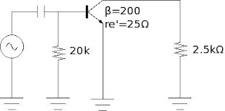
The input impedance $(Z_{in(total)})$ of the common-emitter amplifier given below is:
$5k\Omega$
$4k\Omega$
$2k\Omega$
$20k\Omega$
As $\beta=200$, the value of the transistor base impedance $=\beta(r_e+R_E)=\beta r_e$, since $R_E=0$.
transistor base impedance $=\beta r_e=200\times25=5k\Omega$
$$Z_{in(total)}=20||\beta r_e$$
\begin{align*}
\frac{1}{Z_{in(total)}}&=\frac{1}{20}+\frac{1}{\beta r_e}\\
&=\frac{1}{20}+\frac{1}{5}=\frac{1}{4}
\end{align*}
$$Z_{in(total)}=4k\Omega$$
Hence, answer is (B)
The load voltage in a Zener circuit shown below with $V_z=15V$ is approximately
15 V
10 V
14.3 V
15.7 V
$$V_L=V_Z+V_{BE}=15-0.7=14.3 V$$
$V_{BE}$ negative because it has polarity opposite to that of $V_Z$.
Hence, answer is (C)
A positive clamping circuit is one that clamps:
The positive extremity of the signal to the zero level
The positive extremity of the signal to a positive dc voltage
The negative extremity of the signal to the zero level
The negative extremity of the signal to a positive dc voltage
A circuit that places either the positive or negative peak of a signal at a desired D.C level is known as a clamping circuit. A clamping circuit introduces (or restores) a D.C level to an A.C signal. Thus a clamping circuit is also known as D.C restorer, or D.C reinserted or a baseline stabilizer. The following are two general types of clamping.
Positive clamping occurs when negative peaks raised or clamped to ground or on the zero level i.e., it pushes the signal upwards so that negative peaks fall on the zero level.
Negative clamping occurs when positive peaks raised or clamped to ground or on the zero level i.e., it pushes the signal downwards so that the positive peaks fall on the zero level.
In both cases the shape of the original signal has not changed, only there is vertical shift in the signal
Hence, answer is (C).
A positive logic NAND gate performs same as the negative logic:
XOR gate
OR gate
AND gate
NOR gate
The truth table of positive logic NOR gate is
0
0
1
1
0
0
0
1
0
1
1
0
Now invert all values (as if you place inverters on the two inputs and the one output) to find truth table of negative logic NOR gate:
1
1
0
0
1
1
1
0
1
0
0
1
Which is truth table of positive NAND gate
If $C=0.1\mu F$, $R=3.25k\Omega$ in a phase shift oscillator feedback circuit, then the frequency of oscillation is:
200 kHz
100 Hz
200 Hz
100 kHz
Frequency of phase shift oscillator is
$$f_r=\frac{1}{2\pi RC\sqrt{2N}}$$
where, $R$ is the Resistance in Ohms, $C$ is the Capacitance in Farads, and $N$ is the number of RC stages. In phase shift oscillator feed back circuit there are 3 RC stages.
\begin{align*}
f_r&={\textstyle \frac{1}{2\times3.14\times3.25\times10^{3}\times10^{-7} \times\sqrt{2\times 3}}}\\
&=200 Hz
\end{align*}
Hence, answer is (C)
Load regulation is determined by :
Changes in load current and output voltage
Changes in load current and input voltage
Changes in load resistance and input voltage
Changes in Zener current and load current
Load regulation indicates the change in output voltage due to the change in load current. There is another type of voltage regulation, called line regulation and indicates the change in output voltage due to the change in input voltage.
Hence, answer is (A)
A carrier is simultaneously modulated by two sine waves with modulation indices of 0.3 and 0.4; then the total modulation index is :
A sinusoidal signal of peak to peak amplitude 1V and unknown time period is input to the following circuit for 5 seconds duration. If the counter measures a value (3E8)H in hexadecimal then the time period of the input signal is
2.5 ms
4 ms
10 ms
5 ms
In general n-bit counter counts $2^n$ numbers in a sequence ranging from 0 to $2^n-1$ and the counter cycles through the same sequence of numbers continuously so long as there is an incoming clock pulse. For one complete cycle we require $2^n-1$ pulses.
If $T$ is time period of a pulse then time required for one complete cycle of counts = $T\times(2^n-1)$.
Now, to count a decimal number $N$ we require $N$ pulses. This can be seen from a table below for a 2-bit counter.
Input pulse
Count
decimal equivalent
0
00
0
1
01
1
2
10
2
3
11
3
The decimal equivalent of $(3E8)_H={\scriptstyle 3\times16^2+14\times16^1+8\times16^0}=1000$
Hence, 1000 pulses of time period $T$ will be required to count the number $(3E8)_H$ in 5 seconds.
$$5 \:sec=1000\times T$$
$$T=\frac{5}{1000}=5\:msec$$
Hence, answer is (D)
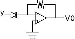
If the parameters $y$ and $x$ are related by $y=\log{(x)}$$, then the circuit that can be used to produce an output voltage
$V_0$ varying linearly with $x$ is
Option (A) is a integrator circuit having output $V_0=-\frac{1}{R*C}\int\limits_0^tV_{in}\:dt$.
Option (B) is a logarithmic circuit having output $V_0=-V_t*\ln{\frac{V_{in}}{I_{d0}R}}$, where $I_{do}$ is reverse saturation current,
Option (C) is a antilog circuit having output $V_0=-I_0*R*e^{ V_{in}/V_t}$, where $V_t$ is the voltage equivalent of temperature
Option (D) is a differentiation circuit having output $V_0=-R*C\frac{dV_{in}}{dt}$.
In our case $V_{in}=\log{(x)}$, hence, clearly, antilog circuit will give desired output
Hence, answer (C) is correct.
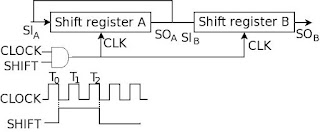
In the schematic figure given below, the initial values of 4 bit shift registers A and B are 1011 and 0010, respectively. The values at $SO_A$ and $SO_B$ after the pulse $T_2$ are respectively
1110 and 1001
1101 and 1001
1101 and 1100
1110 and 1100
Clock pulses will be applied to shift registers A and B, when the SHIFT at input of AND gate is 1. When SHIFT is 1, two clock pulses will be applied to shift registers A and B. When clock pulses appears, the bits of two registers will shift as shown below
Hence, answer is (D)
The high input impedance of field effect transistor (FET) amplifier is due to
the pinch-off voltage
its very low gate current
the source and drain being far apart
the geometry of the FET
The pinch-off voltage
Hence, answer is (A)
The circuit shown in the figure functions as
an OR gate
an AND gate
a NOR gate
a NAND gate
When either or both inputs A and B will be high, the respective transistors will be made ON and output will be high, hence circuit functions as OR gate
Hence, answer is (A)
Considers circuits as shown in figures (a) and (b) below.
If transistors in figures (a) and (b) have current gain ($\beta_{dc}$) of 100 and 10 respectively, then they operate in the
Hence, collector to base junction is reverse biased.
As base to emitter junction is forward biased and collector to base junctions is reversed biased, the transistor is in active region.
Hence, answer is (B)
Ripple factor is defined as the ratio between :
$V_{ac}V_{dc}$
$V_{ac}/V_{dc}$
$V_{dc}/V_{ac}$
$V_{in}/V_{out}$
Ripple factor is defined as the ratio of the root mean square (rms) value of the ripple voltage to the absolute value of the DC component of the output voltage.
Hence, answer is (B)
In the circuit given below, the thermister has a resistance 3 $k\Omega$ at $25^o C$. Its resistance decreases by 150 $\Omega$ per $^oC$ upon heating. The output voltage of the circuit at $30^oC$ is
$-3.75$ V
$-2.25$ V
$2.25$ V
$3.75$ V
Resistance of thermister at $30^oC$ is $R_f=2.25$
\begin{align*}
V_{out}&=-\frac{R_f}{R_i}V_{in}\\
&=-\frac{2.25}{1}(-1)\\
&=2.25\:V
\end{align*}
Hence, answer is (C)
For the logic circuit given below, the decimal count sequence and the modulus of the circuit corresponding to A B C D are (here, J=K=1 locked)
In the T or "toggle" flip-flop both J=1 and k=1 and it changes its output on each clock edge, giving an output which is half the frequency of the signal to the T input.
Clock
A
B
C
D
Decimal
0
1
0
0
0
8
1
0
1
0
0
4
2
0
0
1
0
2
3
1
0
0
1
9
4
0
1
0
1
5
5
0
0
1
1
3
6
1
0
0
0
8
Modulus of a counter, is the number of states that the counter will sequence through before returning back to its original value.
Hence, answer is (B)
The tank circuit of a Hartley oscillator is shown in the figure. If $M$ is the mutual inductance between the inductors, the oscillation frequency is
$\frac{1}{2\pi\sqrt{(L_1+L_2+2M)C}}$
$\frac{1}{2\pi\sqrt{(L_1+L_2-2M)C}}$
$\frac{1}{2\pi\sqrt{(L_1+L_2+M)C}}$
$\frac{1}{2\pi\sqrt{(L_1+L_2-M)C}}$
Frequency of Hartley oscillator is given by
$$f=\frac{1}{2\pi\sqrt{LC}}$$
where $L=L_1+L_2$ if the coils are assumed to be winded on different cores and $L_1+L_2+2M$ if they are winded on a single core.
Hence, answer is (A)
In the given digital logic circuit, $A$ and $B$ form the input. The output $Y$ is
The largest analog output voltage from a 6-bit digital to analog converter (DAC) which produces 1.0 V output for a digital input of 010100, is
1.6 V
2.9 V
3.15 V
5.0 V
For a n-bit DAC
$$V_{out}={\textstyle V_R\left(\frac{b_{n-1}}{2^1}+\frac{b_{n-2}}{2^2}+\cdots+\frac{b_{0}}{2^n}\right)}$$
For a 6-bit DAC
$$V_{out}=\!\!{\textstyle V_R\!\!\left(\frac{b_{5}}{2^1}\!+\!\frac{b_{4}}{2^2}\!+\!\frac{b_{3}}{2^3}\!+\!\frac{b_{2}}{2^4}\!+\!\frac{b_{1}}{2^5}\!+\!\frac{b_{0}}{2^6}\right)}$$
For 1.0 V output of a digital input of 010100
$$1=\!{\textstyle V_R\!\!\left(\frac{0}{2^1}+\frac{1}{2^2}+\frac{0}{2^3}+\frac{1}{2^4}+\frac{0}{2^5}+\frac{0}{2^6}\right)}$$
$$V_R=\frac{16}{5}$$
$$V_{max}\!=\!{\textstyle \frac{16}{5}\!\left(\frac{1}{2^1}\!+\!\frac{1}{2^2}\!+\!\frac{1}{2^3}\!+\!\frac{1}{2^4}+\frac{1}{2^5}\!+\!\frac{1}{2^6}\right)}$$
$$V_{max}=3.15 V$$
Hence, answer is (C)
The low-pass active filter shown in the figure has a cut-off frequency of 2 kHz and a pass band gain of 1.5. The values of the resistors are
$R_1 = 10\: k\Omega$; $R_2 = 1.3 \Omega$
$R_1 = 30\: k\Omega$; $R_2 = 1.3 \Omega$
$R_1 = 10\: k\Omega$; $R_2 = 1.7 k\Omega$
$R_1 = 30\: k\Omega$; $R_2 = 1.7 k\Omega$
Using
$$Gain=1+\frac{15k}{R_1}$$
$$R_1=30\:k\Omega$$
Using
$$f_c=\frac{1}{2\pi RC}$$
$$R=\frac{1}{2\pi f_cC}=1.7\:k\Omega$$
Hence, answer is (D)
The dependence of current $I$ on the voltage $V$ of a certain device is given by $$I=I_0\left(1-\frac{V}{V_0}\right)^2$$
where $I_0$ and $V_0$ are constants. In an experiment the current $I$ is measured as the voltage $V$ applied across the device is increased. The parameters $V_0$ and $\sqrt{I_0}$ can be graphically determined as
the slope and the y-intercept of the $I-V^2$ graph
the negative of the ratio of the y-intercept and the slope, and the y-intercept of the $I-V^2$ graph
the slope and the y-intercept of the $\sqrt{I}-V$ graph
the negative of the ratio of the y-intercept and the slope, and the y-intercept of the $\sqrt{I}-V$ graph
The equation $$I=I_0\left(1-\frac{V}{V_0}\right)^2$$ can be written as
$$\sqrt{I}=-\frac{\sqrt{I_0}}{V_0}V+\sqrt{I_0}$$
Hence, $\sqrt{I}-V$ graph is a straight line with slope $-\frac{\sqrt{I_0}}{V_0}$ and y-intercept $\sqrt{I_0}$
Hence, answer is (D)
In the schematic figure given below, assume that the propagation delay of each logic gate is $t_{gate}$.
The propagation delay of the circuit will be maximum when the logic inputs A and B make the transition
$(0,1)\rightarrow(1,1)$
$(1,1)\rightarrow(0,1)$
$(0,0)\rightarrow(1,1)$
$(0,0)\rightarrow(0,1)$
When input of gate changes its state, the output of gate does not change instantaneously. Instead, the out put changes after a small delay. The delay in the circuit due to all gates is called propagation delay. The states of each gate for different inputs are as shown below.
During transition $(0,1)\rightarrow(1,1)$ from figures (b) and (c) we see that only first OR gate, AND gate, and second OR change their states. Hence, time delay is $3t_{gate}$
During transition $(1,1)\rightarrow(0,1)$ from figures (c) and (b) we see that only first OR gate, AND gate, and second OR change their states. Hence, time delay is $3t_{gate}$
During transition $(0,0)\rightarrow(1,1)$ from figures (a) and (c) we see that only NOT gate changes its state. Hence, time delay is $t_{gate}$
During transition $(0,0)\rightarrow(0,1)$ from figures (a) and (b) we see that all gates change their states. Hence, time delay is $4t_{gate}$
Hence, answer is (D)
Given the input voltage $V_i$, which of the following waveforms correctly represents the output voltage $V_0$ in the circuit shown below?
Output voltage is given by
$$V_0=A(V_2-V_1)$$
where, $V_1$ and $V_2$ are voltages at inverting and non-inverting inputs and $A$ is gain given by
$$A=\frac{R_f}{R_i}=\frac{10}{5}=2$$
$$V_0=2(V_2-V_1)$$
$$V_0=A(0.5-V_1)$$
If $V_1>V_2$, $V_0$ will be negative, but no option have negative voltage.
Hence, $V_1\leq V_2$
Since, $V_2=0.5\: V$, maximum value of $V_1=0.5$, hence, minimum output voltage is $V_{0_{min}}=0$
Also, this is inverting amplifier.
Hence, answer is (B)
Consider an $n$-MOSFET with the following parameters: current drive strength $K= 60 \:\mu A/V^2$, breakdown voltage $BV_{DS}=10\: V$, ratio of effective gate width to the channel length $\frac{W}{L}=5$ and threshold voltage
$V_{th}=0.5V$. In the circuit given below, this $n$-MOSFET is operating in the
ohmic region
cut-off region
saturation region
breakdown region
The MOSFET is in
saturation when $V_{GS} > V_{th}$ and $V_{DS} > V_{GS} - V_{th}$.
cut-off region when $V_{GS} < V_{th}$
linear when $V_{GS} > V_{th}$ and $V_{DS} < V_{GS} - V_{th}$.


 If transistors in figures (a) and (b) have current gain ($\beta_{dc}$) of 100 and 10 respectively, then they operate in the


yyi
ReplyDelete